Progress Report January - April 2022 (What's new in Version 2.3)
Checks improvements
Some users brought up that checks were taking excessively long on their medium-sized board of about 630 components, so I had a look at what could be done to make them faster.
Copper clearance check speedup
By far the most time-consuming check is the copper clearance check as it has to check almost every copper feature against every other one. It does so by offsetting one by the clearance and then calculating the intersecting polygon. Since quite some time now, these checks are being done in parallel to speed things up.
This however left an important optimisation on the table. Offsetting a patch takes significant time on its own, but is being done over and over as patches are checked against each other. To only offset patches once, the copper clearance check now works like this:
- Get patches on copper layers
- Calculate bounding box of each patch (done in parallel)
- Figure out patch pairs, i.e. which patches need to be checked against each other
- Determine which patches need to be expanded by their clearance
- Expand patches by clearance (done in parallel)
- Check each patch pair for whether its patches intersect
After discussing this with Erik, he came up with a pull request that implemented this along with a couple of other optimisations. While the pull request was functional, I had difficulty reasoning about its correctness since it made extensive use of the struct-of-array idiom. Doing so required indexing different vectors with no compile-time guarantee that an index is used for its intended vector.
While bugs in most parts of Horizon EDA are annoying at worst, the copper clearance check is one of the areas where bugs can really ruin one’s day by not catching rule violations that could result in non-functional boards.
To make it easier to reason about the check’s correctness I implemented a vector wrapper that supports strong index types and removed some premature optimisations that had little measurable performance impact. The vector wrapper ensures at compile time that an index can only be used with the intended vectors.
All in all, these optimisations reduced the time it takes to run the checks on that particular board from 8 minutes to about 2½ on my machine.
Cancelling checks
Even more annoying than checks taking excessively long was that there was no way to cancel them other than forcibly terminating the editor, potentially losing unsaved work.
There now is a button to cancel running checks and trying to close the
rules/checks window also cancels any running checks. Cancelling is
implemented by means of an atomic bool variable that’s set from the UI
thread and some if (cancelled) return; statements sprinkled over the
checks.
Check cache mutex thinko
Since most of the board checks need the board flattened into a set of polygons (patches) grouped by net, layer and patch type (pad, track, etc.), that computation is supposed to be done once and used by all checks. As all checks run in parallel, the cache is guarded by a mutex:
RulesCheckCacheBase &RulesCheckCache::get_cache(RulesCheckCacheID id)
{
    if (!cache.count(id)) {
        std::lock_guard<std::mutex> guard(mutex);
        switch (id) {
        case RulesCheckCacheID::BOARD_IMAGE:
            cache.emplace(id, std::make_unique<RulesCheckCacheBoardImage>(core));
            break;
        /*other IDs*/
        }
    }
    return *cache.at(id);
}
I initially put the mutex inside of the if since checking if the id
is already present in the cache shouldn’t require holding a mutex. Thinking about it while writing this blog post, I came to the
opposite conclusion since another thread could have put the cache map
into an inconsistent state while emplacing a cache.
This
however didn’t result in the intended behaviour. Initially, the id
isn’t in the cache, so all checks requesting any cache id will fall
into the if and try to grab the mutex. Whichever is first acquires the
mutex, creates the cache of the requested id, adds it and eventually
releases the mutex. Then, the next check will acquire the mutex,
create the cache, which is then immediately discarded since it’s
already added.
Instead of each cache being calculated once, it gets calculated over and over sequentially for each check!
After recognising this rather embarrassing bug, fixing it was as simple as hoisting the the lock guard to the very top of the method. That way, the first check to acquire the mutex calculates and adds a particular cache and the subsequent checks then find the cache to be there already once they acquire the mutex.
Check status polling
After starting the checks, I noticed that the user interface was getting unresponsive, which came as a surprise since the checks are running in threads outside of the main UI thread. Attaching a profiler and staring at the code revealed that the checks were calling a dispatcher into the main thread for every status update which eventually stalled it.
To prevent this from happening, the main thread now periodically polls the the check status.
More schematic checks
For most of their existence the schematic checks have been rather bare-bones as they only checked for single pin nets. In addition to that, there are now checks for
- single label nets, i.e. nets that only have one net segment with a label attached
- unconnected pins
- unconnected ports
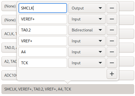
Direction on alternate pin names
Ever since day 0, pins supported multiple names to accurately describe multi-function pins as they’re commonly found on microcontrollers. As it comes with features that are there early on, there’s always the chance of them not being as well thought out as they should have been. In this particular case:
- Alternate names can’t specify direction different from the primary name
- Alternate names are referenced only by index, making it hard to reliably reference them in schematics
To address both of these shortcomings in one go, alternate names are now referenced by UUID (as everything else) and also carry a direction. This also brought us a nicer editor for alternate names:
German umlauts
Horizon EDA uses the Hershey fonts to draw text in everything from symbols to boards. While they contain a number of non-ASCII glyphs such as µ and Ω, they’re missing German umlauts which is rather unfortunate as many users are German-speaking.
The hershey fonts are stored in a rather idiosyncratic format that
encodes numbers as ASCII characters relative to R and ends up looking
a lot like line noise. Naturally, there’s no editor for it. So I hacked up a
really ugly python script that converts between the hershey font
format and SVG paths, to use Inkscape for modifying glyphs. By
pasting the dot from an i on top of a/o/u and integrating them into the character
set, texts now support umlauts. This still leaves the ß, but
designing that to fit within the well-made hershey fonts is beyond my
skills.
Non-modal text editing
As all tools, the “Place text” one started out using modal dialogs that block all other interaction as they’re easier to implement. Now that the interactive manipulator also supports non-modal dialogs in tools, I decided it was about time to use them to enable a richer text editing experience:
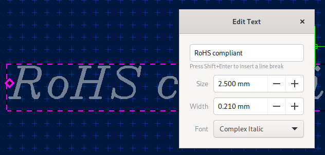
Every change in the dialog is instantly reflected in the text object being edited.
3D preview animations
To make the transitions triggered by the view all/top/bottom/etc. buttons less jarring, these are now smoothed by animations. Same as the smooth zooming, they use a mass-spring-damper system simulation for interpolation.
Non-blocking 3D preview rendering
Opening the 3D preview for the medium-large board I got handed to have look at the checks, I also noticed that opening the 3D preview was blocking the UI unacceptably long.
Instead of the application becoming unresponsive, there now is a pretty loading bar:
On top of that, the layers making up the 3D preview are rendered in parallel.
Plane update progress indication
Another improvement that came out of the board I got handed is that plane updates don’t lock up the user interface anymore. Updating all planes on that particular board blocked the user interface for 30 seconds with no way of cancelling.
To stop the UI from locking up, planes are now updated in a background thread. During that time, the editor grabs all keyboard and mouse input, preventing modifications to the board. If the plane update takes longer than 2 seconds, a dialog that provides progress indication and a way to cancel the the plane update pops up.
This still leaves the possibility for plane update to take 2.1 seconds which will lead to the dialog flashing up just for a split second, leaving the user puzzled if they missed anything.
As that’s not a good user experience either, the board editor stores if the dialog was shown for each board and plane and immediately shows the dialog if it was shown in the last plane update. That way, it’s ensured that the dialog is always visible long enough to be properly recognized by the user.
3D mouse support
A while ago, a friend found a DLR SpaceMouse in the attic. Much to our surprise, it’s still supported by spacenav out of the box with very little configuration, which is quite impressive considering that it’s almost 30 years old. A quick test with the included sample applications confirmed that it’s indeed working.
Naturally, the next thing was to add support for it in the 3D preview. The API provided by libspnav couldn’t have been any simpler: Connect to the spacenav daemon, retrieve the file descriptor and call the method to poll for events whenever data is available on the file descriptor. All that’s left to do was to feed the received deltas into the animators for the corresponding axis to provide some smoothing. All of this took less than 100 lines of code.
All in all, the feature isn’t all that useful, but very fun to play with!
Thermal rules and spoke customisation
Motivated by Issue 618, I had a go at adding more flexibility to thermal relief generation in planes. In addition to specifying the connection style, i.e. solid or thermal relief in the plane itself, we now have thermal relief rules that can override the connection style based on component, pad, layer and net.
While I was at it, I also added support for specifying the number of spokes and their angle.
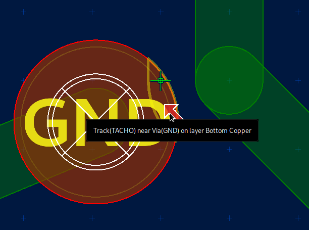
Marker improvements
Filtering
When checks result in many errors, the board can get quite crowded with error markers and error polgons. To reduce clutter, there now are several ways to selectively hide them.
The checks page of the rules window grew a checkbox to only show markers that belong to the currently active layer. This also applies to the error polygons drawn on the board to make it easier to tell which layer an error polygon relates to.
Also, collapsing a rule in the error list now hides its markers and error polygons on the board.
Tooltips
While double-clicking an item in the list of errors centers the marker on screen, there hasn’t yet been a way to find out which error a marker is indicating. To solve that, markers now have tooltips that show their reason for being there.
Net ties
Every now and then, people were asking for ways of joining two nets on the board in one place, such as analog and digital ground. Rather than relying on a workaround based on components, there now are proper net ties.
See the docs for how to use them. I now came to realize that documenting the use of new features in the blog isn’t optimal for discovery and keeping the documentation up to date, so they’re now documented where they should be.
Offset pad connection
For some pad shapes, not connecting the track to the pad origin can be more practical. To support this, while still having the track logically connect to the pad there now is the “Move track connection” tool.
See the docs for how to use it.
Board connectivity check
Up until now, the only check to make sure that all copper features of a net are properly connected was the preflight check checking for airwires. With the addition of the offset pad connection feature however, there could be cases where a track doesn’t connect to a track physically even though it’s connected logically.
To catch these kinds of errors, there now is the board connectivity check that checks that all copper features of a net are actually connected. Most of this check was fairly straightforward to implement by constructing a graph where nodes are copper polygons with zero or more holes and and edges are PTH holes and checking how many connected sub-graphs there are. Properly supporting connections made by the shorted pads rule took a disproportionate amount of effort as the shorted pads rule operates on pads (as the name implies) whereas the check operates on polygons that don’t know if they originated from a pad or something else.
This is a good example how complexity can be multiplicative. Features don’t exist in isolation, so when adding new ones, one also has to make sure that they work well with what’s there already.
ODB++ output
Unless you’re going to etch your PCBs at home, you’ll need to send the board layout to a PCB manufacturer to get them made. The traditional format for this purpose is Gerber. Originally intended as language to drive photo plotters (think G-Code), it turned more and more into a data exchange format.
Apart from Gerber, the only other format that has seen significant use
is ODB++ as far as I’m aware. The wikipedia
article provides a good
overview on its history and origins.
Some time ago, I’ve been approached by users about adding ODB++ output to Horizon EDA since they wanted to import a board they designed into a power integrity simulation application that only supported importing ODB++. By skimming the specification, I deemed that exporting ODB++ was feasible to implement. However, it’s always helpful to have a sample file at hand to verify one’s understanding of the specification. As I couldn’t find any back then, I asked on the EEVBlog forum, but then found more important or fun things to do.
This topic regained my attention when other people also voiced interest in ODB++ export on the forum. Another factor contributing to implementing ODB++ export was me being curios about the format and how it compares to Gerber. There’s certainly no better way to learn about a file format than to implement software the writes it. Checking the ODB++ website once more, I was happy to see that there’s an ODB++ sample design available for download. Equipped with the specification, a sample file and the ODB++ viewer running perfectly in Wine, everything was there to start implementing ODB++ output.
Similar to Gerber, a single ODB++ job is made up of multiple files in a
specific directory structure. Canonically, they’re packed up as a tarball.
To not litter the code with messy file system operations for creating
files and directories as needed, I introduced a
TreeWriter class
that provides an easy to use and hard to misuse interface for the task
and enforces semantics that are compatible with writing to archives
such as only one file being open at once and not re-opening a file
after another file was opened.
It comes in two variants: One that writes to the file system
and one that uses libarchive for
directly writing to a tarball or a zip archive.
The central part of an ODB++ job is the matrix. It’s in
matrix/matrix. I had some difficulty
grasping its purpose initially, but here’s my understanding: ODB++
supports multiple designs in a single job for panelisation. Each
individual design is called a “step” in ODB++. Rows in the matrix
represent layers and each step is its own column.
| Layer↓ / Step → | Design A | Design B |
|---|---|---|
| Top copper | layer image | layer image |
| Bottom copper | layer image | layer image |
The cells of the matrix are then image of each layer for each step. The
image for each layer is described by the features file in the
steps/<step name>/<layer name> subdirectory file. The overall drawing
model is similar to that one used by Gerber, though it carries less
state. In Gerber, one first selects an aperture of certain size and
shape (think pen) and then uses it for drawing lines or pads.
In ODB++, the pen is called symbol and specified by the line itself
rather than being kept in global state. ODB++ specifies a range of
built-in parametrizable symbols for common shapes such as circles or
rectangles. Since specifying the entire symbol name for each line would
be wasteful in terms of file size, each symbol is assigned a unique
integer. Lines and pads then reference the symbol by that
integer rather than its name. For those familiar with X11 or Win32,
this is the same concept as atoms on these platforms.
Custom symbols, as they’re needed for more complex
padstacks, are also supported. They’re defined by the features file
in symbols/<symbol name>. As you might have guessed from the file
name, they use the same format as the layer image itself. This is much
nicer than Gerber’s aperture macros which for example don’t support polygons with
rounded edges at all. Upon re-reading the Gerber spec, I discovered
that it supports so-called “block apertures” since 2015 that can make use of the
drawing primitives available for the board.
To represent planes and polygons, ODB++ uses surface records. These consist of one (or more, though not recommended) contour describing the outline of a polygon and zero or more contours for the holes within the outline. A contour is made up of straight lines and arc segments, a good match for polygons in Horizon EDA. Gerber on the other hand as no notion of holes within polygons. To add a hole inside of a polygon (region in Gerber parlance), one switches the polarity to light, effectively erasing everything that has been drawn in the area of the hole.
Surfaces are also used for defining the outline (profile) of the board
in the steps/<step name>/profile file. The board’s profile is
supposed to be made up of one surface with one outline contour and zero
or more hole contours. This makes it necessary to determine which
polygons on the outline layer are holes and which ones aren’t. For the
3D preview and step export, this was accomplished with clipper by
applying an odd-even fill rule. For the ODB++ export this wasn’t an
option though since clipper can only deal with polygons with straight
contours and outputting arcs approximated by line segments is
outline polygons by finding a polygon that encloses all others.
inaccurate. So I wrote some
code
that tells apart holes from outline polygons. This also directly benefited
the STEP export (see below) and yielded a check that makes sure that
the board outline complies with these requirements.
With all of that implemented, the ODB++ export was about on par with the Gerber one.
The next step was to add nets. Nets are stored in the steps/<step
name>/eda/data file. Each net then has records that point to the
features defined for each layer by index. That way, features are
assigned the net they are connected to.
Other than nets, the steps/<step name>/eda/data file also contains
outlines for packages and their pads or toeprints, as they’re called in
ODB++ parlance. These packages are referenced by the components file
on the special layers comp_+_top and comp_+_bot to indicate the
position of components.
Throughout the ODB++ job, attributes can be attached to features, layers, nets and other objects to add supplemental information such as if a pad is a via or an actual pad or specifying a net’s net class.
Overall, the ODB++ export added about 3000 lines of code and took roughly one month of off-and-on coding. Having implemented both Gerber and ODB++ output in Horizon EDA, I can say that both are adequate formats for exporting PCBs for manufacturing. On To be fair to Gerber, right now, the ODB++ export is more featureful as in knowing about nets and components than the Gerber export since I haven’t implemented the relevant parts of the Gerber spec yet and not because Gerber doesn’t support them. This is mostly due to the Gerber export having been implemented about five years ago back when the rest of Horizon EDA was much less mature and the only goal was to have something to get the application off the ground with no effort spent on any bells and whistles.
Last but not least, Horizon EDA is now listed as ODB++Design Development Partner. To my best knowledge, Horizon EDA is the first free and open-source PCB design tool to implement ODB++ output.
View at actual size action
Many times after receiving boards I designed, I was surprised to see how small they actually are. To get a better idea of their true size, we now have the “View at actual size” action that sets the zoom level such that one millimeter on the board corresponds to exactly that on screen. This relies on Gtk knowing the monitor’s size and resolution, which worked great on my computer so far.
Reflowing tool bar
When introducing configurable key bindings in tools the tool bar showing the available keys got a visual upgrade in the way of giving the keys a more distinct appearance. This however has the downside that list of keys now is a box that just clips its content if the available width is insufficient. Previously, the list of keys was one long label that reflows into multiple lines in that case.
What’s needed to solve this is a container that reflows its children similar to how a label reflows words. Since Gtk doesn’t have such a container built in and asking on the GNOME forum also didn’t yield anything useful, I had to roll my own container.
With the help of DzlColumnLayout which does something similar and the Gtkmm custom container example I managed to implement a container that fit my needs. While I’m not 100% confident that I got everything of Gtk’s intricate geometry management system right, the container seems to work well enough:

Improved board outline in STEP export
Exporting a board whose outline includes polygons with arcs, it occured to me that I was lazy back then and the STEP export flattens arcs in the board outline into line segments. Since the I was working on the ODB++ output in the meantime, I realized that the hard work of figuring out which polygons represent the outline and which ones represent holes was already done, so all that’s left to do was to convert the polygon representation of Horizon EDA to the one from Open CASCADE. As usual Open CASCADE’s documentation on that topic left a lot to be desired. Have a guess which overload’s needed to make a wire in the shape of an arc. Fortunately, KiCad’s step exporter does handle arcs the right way, so I could use their implementation to figure out how get Open CASCADE to do the right thing.
Version 2.3
With all of these improvements and new features, the time is right for
the next release, version 2.3
“Iceblink”.
See the
changelog for a list of
all enhancements and bugfixes included in this release.