Progress Report November 2022 - June 2023 (What's new in Version 2.5)
Blind and buried vias
There are many advanced features a PCB layout tool may or may not have. While there are workarounds for some missing features, you’re out of luck when you need blind or buried vias and your layout tool doesn’t support them.
When starting the development of Horizon EDA, I explicitly decided to not support blind or buried vias to keep things simple and I didn’t expect users to use a new and untested PCB layout tool to make expensive PCBs that need blind or buried vias.
As Horizon EDA matured, users started asking asking for blind and buried vias. This and them being one of the last non-workaroundable features missing, I set out to finally implement support for blind and buried vias.
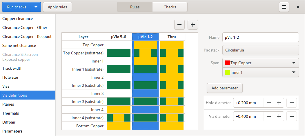
The essence of blind and buried vias is that their hole doesn’t go all
the way through the board. To represent that, the Hole class got a
new member that defines its span, i.e. its start and end layer.
Previously, a (plated) hole implied connectivity across all copper
layers, whereas it’s now required to consider a hole’s span to
determine which layers it connects. The patch canvas used for design
rule checks and 3D preview also required some essential
changes since
there are now patches that span multiple layers. Before the
introduction of blind and buried layers, the only-multi-layer patches
were plated and non-plated through holes. As an implementation
shortcut, they were placed on the layer 10000 which lead to various
implementation quirks to handle this special case. By using a
LayerRange, single- and multi-layer patches are now handled in a
unified way.
The ODB++ and gerber export naturally required changes as well to support individual drill layers for every span. Implementing this in the ODB++ export didn’t require any changes to the user interface since an ODB++ job contains all required metadata to specify the span of dril layers. The gerber export however required some UI to specify the drill filenames similar to the layer filenames.
Overall, this added just a little less than 1000 lines of code.
Via definitions
Before designing a board that uses blind and buried vias, one usually agrees on a stackup with the board manufacturer that specifies which via spans will get made.
To reflect this in Horizon EDA, we now have the via definition rule to specify which kinds of non-through vias can be used.
See the docs for how to use via definitions.
Undo/redo enhancements
A while ago, I came across a nice article about the problem that editing while redo is possible clears the redo stack. This felt very relatable and the article offered a fairly easy to implement a undo/redo redo behaviour that never loses anything, so I went ahead and implemented it. To use it, enable “Undo/redo that never forgets” in the preferences.
One of the nice aspects of developing Horizon EDA is that one can quickly go from “it’d be nice if…” to “that’s nice” when it comes to features like these.
Part, Entity and Unit editor enhancements
In Horizon EDA, parts can inherit from other parts to represent components that are electrically identical and only differ in some parameters such as MCUs with varying amount of memory. Up until now, there was no way in the UI to change a part’s base part. Doing so can be convenient when creating a part that’s a member of a larger series, but being too lazy to create the base part before creating the actual part. To simplify this particular use case, the part editor now can create a base part that’s a copy of the current part and set the current part to inherit everything from the base part in one single action.
To keep implementation complexity low (i.e. laziness) the part, unit, and entity editors only supported updating the user interface from the to-be edited once on startup. This had to change for the part editor to support changing the current part to inherit everything from the base part. With this obstacle out of the way, adding undo/redo to the part editor became fairly easy. For consistency and completeness, the entity and unit editor now support undo/redo as well.
Pin names search
Horizon EDA supports multiple functions per pin to properly represent multiplexed pin functions as they’re common on MCUs. Since MCUs have many pins with many functions, it’s a bit tedious to find the pin that has the right function in the select pin names dialog. To make them easier to find, it grew a search bar.
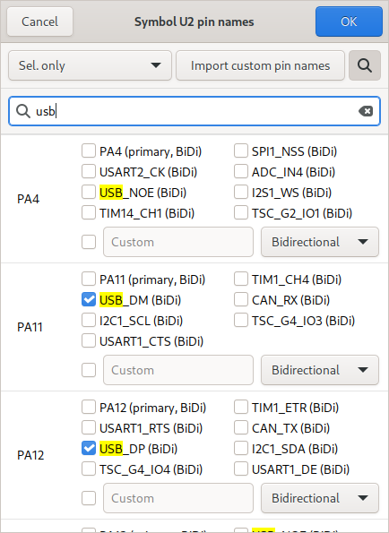
Adding the search was fairly simple, but highlighting the search string in the checkboxes took a disproportionate amount of code.
Gerber plane export bugfixes
In the process of exporting a board to Gerber, Horizon EDA maps its drawing model to the one from Gerber and has to paper over the resulting impedance mismatches. For tracks, that’s fairly easy as there are only so many ways of representing lines on a 2D plane.
For planes however, the situation is a bit more involved. In Horizon EDA, planes are composed of fragments. A fragment is a polygon with zero or more holes with the outline and holes defined by their contour. Gerber on the other hand, doesn’t support polygons with holes. Instead, it supports polygons, regions in Gerber parlance, of light and dark polarity. A dark polarity region draws over everything that was drawn before and a light polarity region erases everything underneath it. So to represent a fragment with holes, Horizon EDA first draws the outline in dark polarity followed by the holes in light polarity.
While this seems simple enough for one fragment, this approach falls apart when a plane with a hole in it is surrounded by another plane and the surrounding plane has a fragment inside the hole of the first plane. The fragments would get added to the Gerber image in that order:
- Outline of the outer plane
- Hole of the outer plane
- Fragment inside of the hole of the outer plane
- Outline of the inner plane
- Hole of the inner plane
The bug is that the hole of the inner plane erases the fragment of the outer plane.
To resolve this bug, all fragments of all planes on a single layer get processed by Clipper’s polytree to correctly establish which fragment exists in which hole. Fragments are then drawn in such order that everything existing inside a hole gets drawn after the hole has been drawn using light polarity.
Pool reload enhancements
Reloading the pool in the schematic, board or any other editor used to clear the undo/redo history since the pool items pointed to by the copies on the undo/redo stack are gone after clearing the pool to reload it.
To remove this limitation, all items from the pool are now handled as
shared_ptrs so that they’ll be around as long as needed and are not
affected by clearing the pool.
Select plane at cursor
While debugging the issues related to gerber export of planes, I frequently had a hard time figuring out which plane I was looking at. Since the computer has a less hard time figuring this out, there now is an action that selects the plane that’s under the cursor.
Version 2.5
Finally, version 2.5 “Kepler” is out! See the changelog for a list of all enhancements and bugfixes included in this release.
This took a bit longer than initially planned, but I really wanted to get blind an buried vias into this release and then got distracted by various other projects.
Also keep in mind that Horizon EDA is mostly a one-person show that I run in my spare time, so bear with me if things take a little longer.